Why do ceramic substrate PCB processing require laser processing equipment more?
2020-06-11


The laser processing equipment for ceramic substrate PCB is mainly used for cutting and drilling. Due to the many technical advantages of laser cutting, it has been widely used in the precision cutting industry. Let's take a look at the advantages of laser cutting technology in PCB.
1. Laser Processing Technology and Ceramic Substrate PCB
With the continuous advancement of 5G construction, the precision microelectronics and aerospace industries have further developed, and these fields all involve the application of ceramic substrates. Among them, ceramic substrate PCB has gradually gained more applications due to its superior performance.
Ceramic substrates are the basic materials for high-power electronic circuit structure technology and interconnection technology. They are dense in structure and have a certain brittleness. Traditional processing methods generate stress during the processing, which can easily lead to breakage for very thin ceramic sheets.
Under the trends of lightweight and miniaturization, traditional cutting methods can no longer meet the demands due to insufficient precision. Laser is a non-contact processing tool, which has obvious advantages over traditional processing methods in cutting technology, playing a very important role in ceramic substrate PCB processing.
With the continuous development of the microelectronics industry, electronic components are gradually moving towards miniaturization and lightweight, with increasing precision requirements. This inevitably raises higher demands for the processing of ceramic substrates. From the development trend, the application of laser processing for ceramic substrate PCB has broad development prospects!
2. Advantages and Analysis of Laser Processing for Ceramic Substrate PCB
Ceramic materials have good high-frequency performance and electrical properties, as well as high thermal conductivity, chemical stability, and thermal stability, making them ideal packaging materials for producing large-scale integrated circuits and power electronic modules. Laser processing of ceramic substrate PCB is an important application technology in the microelectronics industry. This technology is efficient, fast, and accurate, with high application value.
Advantages of Laser Processing for Ceramic Substrate PCB:
1. Due to the small spot size and high energy density of lasers, the cutting quality is good and the cutting speed is fast;
2. The cutting gap is narrow, saving materials;
3. Laser processing is fine, with smooth and burr-free cutting surfaces;
4. The heat-affected zone is small.
Ceramic substrate PCB is more prone to breakage compared to fiberglass boards and requires higher technical requirements, so laser drilling technology is usually adopted.
Laser drilling technology offers advantages such as high precision, fast speed, high efficiency, scalable mass drilling, applicability to most hard and soft materials, and no tool wear. It meets the requirements for high-density interconnection and fine development of printed circuit boards. Ceramic substrates utilizing laser drilling technology exhibit high bonding strength between ceramic and metal, with no peeling or bubbling, achieving a cohesive growth effect. The surface flatness is high, with roughness ranging from 0.1 to 0.3μm, and the laser drilling diameters range from 0.15 to 0.5mm, with the capability to achieve precision as fine as 0.06mm.
Differences in Cutting Ceramic Substrates with Different Light Sources (UV, Green, Infrared)
Difference 1:
Infrared fiber laser cutting of ceramic substrates uses a wavelength of 1064nm, green light uses a wavelength of 532nm, and ultraviolet uses a wavelength of 355nm.
Infrared fiber lasers can achieve higher power, but the heat-affected zone is also larger;
Green light is slightly better than fiber lasers, with a smaller heat-affected zone;
Ultraviolet lasers operate by breaking molecular bonds in materials, resulting in the smallest heat-affected zone. This is why green light processing may cause slight carbonization during the cutting of non-metal PCB circuit boards, while ultraviolet lasers can achieve minimal or even no carbonization.
Difference 2:
Ultraviolet laser cutting machines can handle FPC soft board cutting, IC chip cutting, and some ultra-thin metal cutting in the PCB field, while high-power green laser cutting machines can only cut PCB hard boards. Although they can also cut FPC soft boards and IC chips, the cutting effect is far inferior to that of ultraviolet lasers.
In terms of processing effects, ultraviolet laser cutting machines are cold light sources, resulting in less heat impact and more ideal effects.
The cutting of PCB circuit boards (non-metallic substrates, ceramic substrates) uses a galvanometer scanning mode to peel layer by layer to form cuts, with high-power ultraviolet laser cutting machines becoming the mainstream market in the PCB field.
Application Cases
1. Han's Laser
Han's Laser ceramic laser cutting machines are mainly used for laser cutting, scribing, and drilling of ceramic materials such as alumina, aluminum nitride, and cobalt oxide.
Cutting samples are as follows:
2. SHINHOP Laser
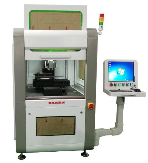
SHINHOP Laser ceramic laser cutting and drilling machines are equipped with imported ITF high-power lasers, with dynamic focus automatic compensation and air cooling functions for the laser cutting head;
Ceramic substrates or thin metal sheets with a thickness of less than 2mm can be cut and drilled, with a minimum hole diameter of 100μm (this equipment is primarily exported to Russia and India).
Cutting samples are as follows:

[This article is referenced from "ACT Laser Gathering" for reference and learning purposes only. If there is any infringement, please inform for handling.]
About Us
Shenzhen SHINHOP Laser Equipment Co., Ltd. It is a scientific and technological enterprise specializing in the research and development, production and sales of industrial laser processing equipment. It has been deeply engaged in the new energy industry for 20 years, focusing on the non-standard customization of automatic lithium battery cell assembly line and module PACK production line. It has successively obtained the national high-tech and specialized new enterprise certification.
Contact Us
Company Address:Building 6, Jingneng Science and Technology Environmental Protection Industrial Park, No.3 Baolong 2nd Road, Longgang District, Shenzhen City, Guangdong Province
Customer service hotline:18898357350
Customer service E-mail:info@shinhop.com
Related News

2026-06-11


Contact Details

Hotline


Address
Building 4, Jingneng Technology and Environmental Protection Industrial Park, 3 Baolong 2nd Road, Longgang District, Shenzhen, Guangdong Province,China

YouTube

TikTok